
Different Types of Circuit Boards
Printed circuit boards are the foundation of many modern computers and computerized devices. Although a simple concept, PCBs are complex structures that can be difficult to repair if they are damaged. This article will explore the history and technology behind these important components.
In 1903, German inventor Albert Hanson patented a device that was the precursor to the modern PCB. His design used conductive wires that were etched on to an insulated board, and the result was what we now call a circuit board. Hanson's invention didn't see widespread use, however, until World War II. During that conflict, the U.S. Army Signal Corps managed to develop a method of printing wires directly onto the insulating surfaces of printed circuit boards, which would greatly increase production speed and allow for much smaller devices. This method was called proximity fuses, and it allowed artillery shells to be guided towards their targets on land and sea by radio signals.
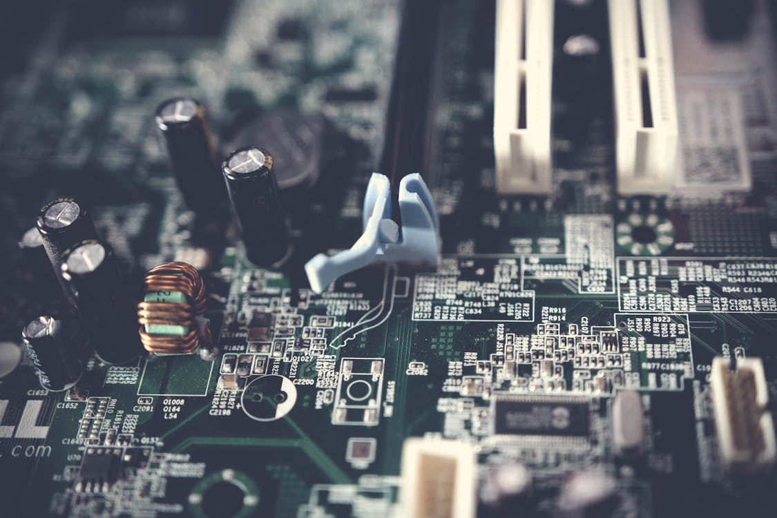
How do circuit boards work, PCBs can be single-sided or double-sided, and they can contain either through-hole or surface mount components. Through-hole mounting involves putting the metal leads of the component into holes that have been drilled into the bare circuit board and soldered in place, while surface mount components are attached by their copper leads to the traces on the other side of the insulating material.
The first step in the creation of a PCB is to make a insulating substrate out of a dielectric composite. This is typically made out of a phenolic cotton paper impregnated with epoxy resin, but it can also be made out of fiberglass or other materials. The insulating properties of the composite are determined by the type and concentration of filler added to it. Common fillers include polytetrafluoroethylene (Teflon), FR-4 glass epoxy, FR-5, FR-6, CEM-1 and CEM-3.
Once the insulating substrate is made, the PCB's artwork pattern is printed on it using a process similar to a photolithographic printer. The areas that have not been printed with the image are covered with a resist material that protects them from being dissolved by the etching solution used to create the circuit patterns on the board. The exposed copper is then etched to reveal the wiring paths, and the board is cleaned to remove any residue from the manufacturing process.
Most modern PCBs are constructed of multilayer boards with copper layers alternating with the substrate layer. This allows for much higher component density and helps prevent circuit traces from crossing each other, which can cause interference and reduce efficiency. In order to maintain quality control, several testing procedures are used during the manufacture of a PCB. These can include visual inspection, automated optical inspection, power-off analysis and in-circuit test. In-circuit test checks whether the PCB functions as designed, and identifies any issues that need to be addressed. Once the testing and etching are complete, the circuit board can be assembled into its final product. It can then be connected to a power supply and tested again.